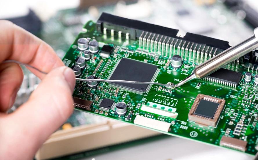
Printed Circuit Boards are easily swayed structures. The fundamental framework of contemporary electronics relies on PCBs and the impeccable manufacturing and subsequent troubleshooting of PCB boards is essential for rightful device behavior. PCB board troubleshooting is the systematic process of discovering, analyzing, and resolving issues within the process of manufacturing of PCB board or the finalized product. In defiance of pivotal function PCBs play, many predicaments are confronted with throughout the process of manufacturing of PCBs having the potential to cause device failure. Consequently, it becomes indispensable to troubleshoot PCB boards to preserve integrity of electronics devices and participate minimalistically in system failure. Troubleshooting PCB circuits calls for knowledge of subject matter, skillfulness, expertise in field and mandates meticulous strategies. A number of issues encountered by PCB manufacturers while designing and fabricating PCBs are in need of swift and proficient troubleshooting techniques.
Henceforth, regular implementation of comprehensive inspections and quality checks are critical for diagnosing any fault in PCB boards followed by application of suitable troubleshooting methods. By PCB board troubleshooting and rectifying issues in the initial stages of manufacturing, the threat of device failure is evidently reduced. Enumerated below are some common issues faced during PCB fabrication along with a review of how to troubleshoot PCB board issues and conduct reliable solutions for resolution.
2. Common Issues in PCB and Their Troubleshooting Methods
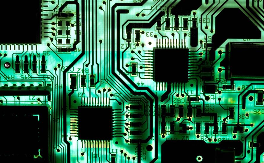
1. Trace widths: Trace width corresponds to the width of conductive paths made of copper on PCB board. Traces are responsible for carrying currents across PCBs and the width of a copper path is responsible for the rating of its current-carrying capacity.
- PCB Issue: Width of traces and distance between consequently placed copper paths has paramount importance during operation of a device. If traces are too narrow and lie too closely with each other, problems like short-circuits, less current carrying capacity than intended, interference between signals and reduced signal integrity are inevitable to arise.
- PCB troubleshooting: Methodical PCB board troubleshooting steps encompassing reviewing original PCB design, thorough check for short-circuits and discontinuity, use of multi-meter or other current-measuring devices to determine current-carrying capacity, employing oscilloscopes for checking signal integrity and modifying trace widths and spacing using specialized PCB design softwares are crucial for mitigating any potential issues.
2. Open circuits/ Short Circuits: Open circuit is a break in traces blocking the flow of electrical currents while short circuit is an unintended connection between two or more traces.
- PCB Issue: Open and short circuits are responsible for discontinuity of flow of electrical current. In the absence of suitable current delivery, components malfunction and pose a threat of burning, subsequently resulting in device failure.
- PCB troubleshooting: To address and troubleshoot this PCB board challenge, primary action involves using a multi-meter and check for all the discontinuities on PCB board. In the instance of open circuits, soldering needs to be fixed in order to provide a clear path for the transfer of current. Should a short circuit occur, the joining area should be cleared foremost of all the conducting material either using a soldering iron or a de-solder pump. Afterward, proper traces are constructed on it with suitable spacing between traces.
3. Material selection: Manufacturing materials of PCB have a noteworthy impact on the efficiency, endurance, holistic functionality, and sustainability of any electronic item. Performance issues arise as a result of incompatibility between system requirements and materials in use. Thus, a worthy compromise between cost of high-quality materials and performance requirements results in identifying suitable materials for a given project.
- PCB Issue: Opting for materials capable of inefficiency in the operation of a device can bring about detrimental problems or even complete failure of an electronic set-up.
- PCB troubleshooting: Addressing the problems associated with material selection can be primarily done by examining the specifications mentioned in design requirements of PCB board. After selecting materials compatible with intended operating environment, tests need to be done to enhance alignment between requirements and material properties. Incompatible materials need to be replaced with proper materials. Furthermore, incorporating trusted manufacturers in the fabrication process can culminate helpful results.
4. Soldering problems: Problems caused during soldering manifest in many ways such as cold solder iron leading to weak connections, incomplete fusion of copper and solder wire, ineffective use of soldering equipments, overheating of solder-iron resulting in bulky connections.
- PCB Issue: Poor soldering leads to intermittent connections thus reducing the transfer rate of currents across PCB board. It does not only cause short circuits and open-circuits problems but hampers the overall functionality of electronic devices.
- PCB troubleshooting: Thorough examination of solder joints and continuity across the board using multi-meter ensures overall troubleshooting PCB circuits of soldering problems. Besides that, learning proper soldering techniques, working on optimal temperature, use of proper amount of flux and deploying high quality instruments have a paramount importance in reducing these issues.
5. Plating voids: Plating voids are air pockets that take place due to insufficient deposition of plating material in the plated-through holes (vias) responsible for connecting different layers of a multi-layer PCB. Using inappropriate amounts of material leads to gaps or empty spaces in the holes causing breaks in electrical connections thus hampering the overall conductivity of PCB.
- PCB Issue: The main issue stemming from plating voids in the introduction of breaks in the flow of across the multi-layers of a PCB board. This phenomenon leads to open circuits, resulting in absolute cessation of PCB operation. It results due to impurities present in the plating material, non-proper plating application, and fluctuations in parameters like temperature, current or time during plating process.
- PCB troubleshooting: to keep this issue in check, visual inspection tools such as magnifying devices are used to find and access plating voids. To modify process inconsistencies, variable parameters such as current density, time, temperature are perfected. Moreover, X-rays are inculcated in PCB board troubleshooting process to detect hidden voids and process validation checks, material selection process and plating baths are scrutinized to ensure the continuity of conducting paths across vias.
6. Incorrect component placement: PCB typically constructs the foundation of electronic devices. It is a board over which different electronic components are mounted as per layout given by PCB engineer.
- PCB Issue: Incorrect component placement on PCB board results in adoption of unnecessary wiring between two joints. PCB board’s appearance should look dapper and tidy, serving not only aesthetic goals but to facilitate the troubleshooting of devices.
- PCB troubleshootingg: This is a frequent problem in PCB manufacturing and troubleshooting PCB circuits demands cross-check of position of each component against the schematic design. Should the need arise, components must be re-soldered and repositioned. Additionally, collaborating with subject matter experts to optimize the positioning of components is an up-to-the-minute approach to tackle this issue.
7. Acid traps: Acid traps are caused by interaction between sharp and narrow corners of copper traces with etching materials causing trace damage and unwanted gaps.
- PCB Issue: Unwanted gaps and damage of copper traces lead to discontinuity in the PCB board, quality degradation, causing signal integrity issues and increased failure rates of PCB boards.
- PCB troubleshooting: Sharp corners should be inspected using magnifying tools and rounded off by filleting. Optimizing etching process by controlling parameters like temperature, concentration of chemicals, controlled spraying, opting for a layout less prone acid-traps and regular inspections are pivotal in hindering the occurrence of acid-traps.
8. Sub-standard components: The electronic constituents utilized in production of PCB boards are the central figures in a PCB, in charge of all the required functions and operations. Incorporation of sub-standard components jeopardizes not only product quality but also sets up a direct path for the potential product failure in the market.
- PCB Issue: Using third-quality components leads to altogether failure of a device or product. Component selection should be guided by the idea of fostering prolonged operational long-time functionality. Inferior quality components may serve their purpose temporarily but are vulnerable to all sorts of issues like overheating, burning, fire hazards, short circuits, ultimately compromising the overall efficiency and functionality of the device.
- PCB troubleshooting: To identify sub-standard elements, conduct a meticulous inspection of all the items. Integrate frequent testing of components in use. Indulging with a single supplier for an extended duration may lead to inconsistency of quality. Engaging a dependable supplier familiar with the technological advancements need to be considered.
9. Overheating: Overheating is a common issue faced across the realm of electrical and electronics domain. Overheating is caused by energy loss during conduction of electrical currents. Each device and equipment have a heat rating that needs to be exercised properly.
- PCB Issue: Components and PCB boards tend to overheat during operation due to transfer of currents from one point to another. Overheating is customarily responsible for device failure.
- PCB troubleshooting: Heat ratings of devices in use should be verified to avoid this issue. To improve the PCB board troubleshooting process, additional components like heat sinks need to be employed.
10. Electrical performance: Adherence to electrical specifications of PCB board determines the effectiveness and reliability of electrical parameters within a circuit. This ensures the presence of appropriate impedance values, less signal distortion, greater signal integrity and negligible data corruption.
- PCB Issue: Compromised performances of impedance matching, and signal integrity are a major reason for PCB failure. These issues often arise as a result of copper trace irregularities and by using sub-standard components and materials in the fabrication of a PCB board.
- PCB troubleshooting: Troubleshooting electrical PCB issues are needful of optimizing design layouts ensuring proper spacing between conducting traces and proper component placement, employing specialized equipments for measuring signal integrity and impedance values and adopting correcting measures.
11. Drilling issues: Holes are made in PCBs to hold components on board, for soldering purposes, for managing various layers of a multi-layer PCB. These are made by using special drilling machines at specific positions by consulting PCB design layout.
- PCB Issue: Common issue that arises due to drilling is misalignment between component position and location of hole. It arises when the drilling process has not been precise and accurate. Another common issue that is confronted is mismatched hole sizes or irregularities in hole walls.
- PCB troubleshooting: Inspecting the tips of drill machines, prompt maintenance of equipments required, and use of proper filing tools are some needful ways to troubleshoot this problem. Also, to ensure the precise positioning of holes, it is imperative to keep an eye on PCB design guidelines during the entire process.
12. Copper to edge clearance: It refers to the distance between outer-most copper traces and edges of PCB board. It has high significance in gauging the effectiveness of a PCB board.
- PCB Issue: If copper-to-edge clearance is insufficient, it implies copper paths designed for carrying currents lie closely with the edge of board and are at an elevated risk of reacting with environmental impurities leading to corrosion. This adjacency also poses a threat of damage for copper traces during assembling of devices.
- PCB troubleshooting: This issue can be addressed by verifying the design rules and reviewing the guidelines mentioned in PCB design for this parameter. If the issue is rooted in fundamental PCB layout, the traces need to be readjusted for a better copper to edge clearance. Additionally, components can be repositioned for a better and effective resolution.
13. Power/ Ground planes: Power and ground planes are responsible for delivering the main power supply to all the layers and components present in a PCB board.
- PCB Issue: The power supply, akin to the Heart of a device, pumps with electrical currents analogous to blood and supplies currents to all the working devices. Obstacles in the delivery of power and ground supply greats play with the functionality, efficiency, and swiftness of a device. If a device or any electronic structure is deprived of main supply, it stands as good as non-operational raw material.
- PCB troubleshooting: A number of measures can be employed to rectify this issue. To start with, a multimeter is deployed to check for continuity and ground traces on the PCB. Next, short/open circuits are inspected manually or by using thermal cameras. Finally, it needs to be ensured that all components are properly connected with the supplies without any loose connections.
14. Environmental factors: Environmental factors including the presence or absence of different conditions and elements serve an impactful role in figuring out the error-free manufacturing of PCB. PCBs are very much vulnerable to the environment and are easily flawed by the presence of any unwanted materials.
- PCB Issue: Dubious and sub-standard environmental conditions like presence of dust, moisture, ion, humidity, chemicals etc. in the manufacturing lab is responsible for altering quality and robustness of a PCB board. Impurities combine with copper traces, silkscreen layers or other alloys used in PCB boards leading to rust, corrosion, and damage of PCB boards.
- PCB troubleshooting: Cleanliness of environment and making sure all the environmental conditions are top-notch and controlled, is the only way to tackle this issue. PCB manufacturing labs should not have any excess moisture, humidity, dryness, heat or cold and should be free from any material that can tamper with PCBs.
Conclusion
In this article, we talked about the common issues in printed circuit board fabrication and how to troubleshoot PCB boards. We hope this will be helpful to you in solving the problems during your PCB fabrication and assembly process or in usage. Please contact us freely if you have any questions about printed circuit boards issues.